- 您现在的位置:买卖IC网 > Sheet目录3875 > DSPIC30F3014T-20I/ML (Microchip Technology)IC DSPIC MCU/DSP 24K 44QFN
dsPIC30F Flash Programming Specification
DS70102K-page 44
2010 Microchip Technology Inc.
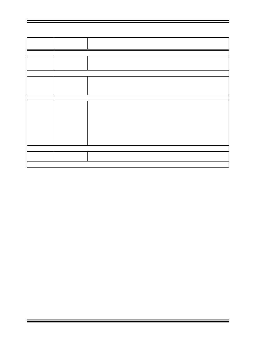
Step 6: Write the Configuration register data to the write latch and increment the write pointer.
0000
BB1B96
000000
TBLWTL W6, [W7++]
NOP
Step 7: Unlock the NVMCON for programming.
0000
200558
883B38
200AA9
883B39
MOV
#0x55, W8
MOV
W8, NVMKEY
MOV
#0xAA, W9
MOV
W9, NVMKEY
Step 8: Initiate the write cycle.
0000
—
0000
A8E761
000000
—
000000
A9E761
000000
BSET NVMCON, #WR
NOP
Externally time ‘P12a’ ms (see Section 13.0 “AC/DC Characteristics and
NOP
BCLR NVMCON, #WR
NOP
Step 9: Reset device internal PC.
0000
040100
000000
GOTO 0x100
NOP
Step 10: Repeat steps 3-9 until all 7 Configuration registers are cleared.
TABLE 11-7:
SERIAL INSTRUCTION EXECUTION FOR WRITING CONFIGURATION
REGISTERS (CONTINUED)
Command
(Binary)
Data
(Hexadecimal)
Description
发布紧急采购,3分钟左右您将得到回复。
相关PDF资料
PIC16LF819T-I/MLTSL
IC PIC MCU FLASH 2KX14 28QFN
PIC16LF819T-I/SOTSL
IC PIC MCU FLASH 2KX14 18SOIC
PIC18LF8410T-I/PT
IC PIC MCU FLASH 8KX16 80TQFP
PIC18F2410T-I/ML
IC PIC MCU FLASH 8KX16 28QFN
PIC18F2331T-E/SOG
IC PIC MCU FLASH 4KX16 28SOIC
PIC18F4331T-I/ML
IC MCU FLASH 4KX16 44QFN
PIC16F690-I/ML
IC PIC MCU FLASH 4KX14 20QFN
PIC16C56A-04I/P
IC MCU OTP 1KX12 18DIP
相关代理商/技术参数
DSPIC30F3014T-20I/PT
功能描述:IC DSPIC MCU/DSP 24K 44TQFP RoHS:否 类别:集成电路 (IC) >> 嵌入式 - 微控制器, 系列:dsPIC™ 30F 产品培训模块:XLP Deep Sleep Mode
8-bit PIC® Microcontroller Portfolio 标准包装:22 系列:PIC® XLP™ 18F 核心处理器:PIC 芯体尺寸:8-位 速度:48MHz 连通性:I²C,SPI,UART/USART,USB 外围设备:欠压检测/复位,POR,PWM,WDT 输入/输出数:14 程序存储器容量:8KB(4K x 16) 程序存储器类型:闪存 EEPROM 大小:256 x 8 RAM 容量:512 x 8 电压 - 电源 (Vcc/Vdd):1.8 V ~ 5.5 V 数据转换器:A/D 11x10b 振荡器型:内部 工作温度:-40°C ~ 85°C 封装/外壳:20-DIP(0.300",7.62mm) 包装:管件 产品目录页面:642 (CN2011-ZH PDF) 配用:DV164126-ND - KIT DEVELOPMENT USB W/PICKIT 2DM164127-ND - KIT DEVELOPMENT USB 18F14/13K50AC164112-ND - VOLTAGE LIMITER MPLAB ICD2 VPP
dsPIC30F3014T-30I/ML
功能描述:数字信号处理器和控制器 - DSP, DSC 44LD 30MIPS 24 KB RoHS:否 制造商:Microchip Technology 核心:dsPIC 数据总线宽度:16 bit 程序存储器大小:16 KB 数据 RAM 大小:2 KB 最大时钟频率:40 MHz 可编程输入/输出端数量:35 定时器数量:3 设备每秒兆指令数:50 MIPs 工作电源电压:3.3 V 最大工作温度:+ 85 C 封装 / 箱体:TQFP-44 安装风格:SMD/SMT
dsPIC30F3014T-30I/PT
功能描述:数字信号处理器和控制器 - DSP, DSC 30MIPS 24 KB RoHS:否 制造商:Microchip Technology 核心:dsPIC 数据总线宽度:16 bit 程序存储器大小:16 KB 数据 RAM 大小:2 KB 最大时钟频率:40 MHz 可编程输入/输出端数量:35 定时器数量:3 设备每秒兆指令数:50 MIPs 工作电源电压:3.3 V 最大工作温度:+ 85 C 封装 / 箱体:TQFP-44 安装风格:SMD/SMT
DSPIC30F4011-20E/ML
功能描述:数字信号处理器和控制器 - DSP, DSC 16 Bit MCU/DSP 44LD 20M 48KB FL RoHS:否 制造商:Microchip Technology 核心:dsPIC 数据总线宽度:16 bit 程序存储器大小:16 KB 数据 RAM 大小:2 KB 最大时钟频率:40 MHz 可编程输入/输出端数量:35 定时器数量:3 设备每秒兆指令数:50 MIPs 工作电源电压:3.3 V 最大工作温度:+ 85 C 封装 / 箱体:TQFP-44 安装风格:SMD/SMT
DSPIC30F4011-20E/P
功能描述:数字信号处理器和控制器 - DSP, DSC 16 Bit MCU/DSP 40LD 20M 48KB FL RoHS:否 制造商:Microchip Technology 核心:dsPIC 数据总线宽度:16 bit 程序存储器大小:16 KB 数据 RAM 大小:2 KB 最大时钟频率:40 MHz 可编程输入/输出端数量:35 定时器数量:3 设备每秒兆指令数:50 MIPs 工作电源电压:3.3 V 最大工作温度:+ 85 C 封装 / 箱体:TQFP-44 安装风格:SMD/SMT
DSPIC30F4011-20E/PT
功能描述:数字信号处理器和控制器 - DSP, DSC 16 Bit MCU/DSP 20M 48KB FL RoHS:否 制造商:Microchip Technology 核心:dsPIC 数据总线宽度:16 bit 程序存储器大小:16 KB 数据 RAM 大小:2 KB 最大时钟频率:40 MHz 可编程输入/输出端数量:35 定时器数量:3 设备每秒兆指令数:50 MIPs 工作电源电压:3.3 V 最大工作温度:+ 85 C 封装 / 箱体:TQFP-44 安装风格:SMD/SMT
DSPIC30F4011-20I/ML
功能描述:数字信号处理器和控制器 - DSP, DSC 16 Bit MCU/DSP 44LD 20M 48KB FL RoHS:否 制造商:Microchip Technology 核心:dsPIC 数据总线宽度:16 bit 程序存储器大小:16 KB 数据 RAM 大小:2 KB 最大时钟频率:40 MHz 可编程输入/输出端数量:35 定时器数量:3 设备每秒兆指令数:50 MIPs 工作电源电压:3.3 V 最大工作温度:+ 85 C 封装 / 箱体:TQFP-44 安装风格:SMD/SMT
DSPIC30F4011-20I/ML
制造商:Microchip Technology Inc 功能描述:16- Bit Digital Signal Controller Memory